


Covid-19 demonstrated the world’s dependance on semiconductors. Even as major chip fabrication units, or fabs, continued operating as essential infrastructure, disruptions across logistics, materials, assembly and testing, combined with demand swings, took a toll on availability. The shortage rippled through sectors ranging from consumer electronics and automobiles to industrial equipment and national defence, laying bare the chinks in global supply chains.
Indian industry, too, felt the impact. It was against this backdrop that Arun Ramchandani, Head of L&T Precision Engineering and Systems, called his old classmate and long-time friend Sandeep Kumar, a 42-year veteran of the semiconductor industry. Ramchandani posed a simple question: What could they do for India?
What followed was nearly two years of discussions, refinements and multiple iterations of plans presented to L&T’s leadership. Finance and marketing teams worked on their own strategies in parallel. By late 2023, a clear direction had emerged.
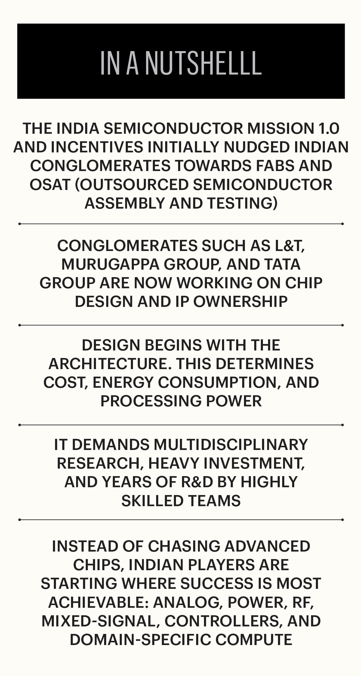
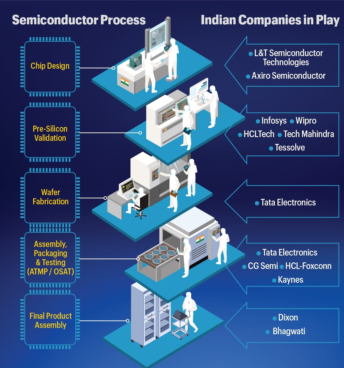
L&T chose to tread a different path from chip fabs or outsourced semiconductor assembly and testing (OSAT). In November 2023, it founded L&T Semiconductor Technologies Ltd (LTSCT). The mandate was a laser focus on designing chips. “Product is where the IP (intellectual property) is, product is where the differentiation is,” says Kumar, Chief Executive of LTSCT. “Once we sell enough products, we will build factories to make those products.”
L&T is not alone. Encouraged by India’s semiconductor push that emphasises building chip fabs and backend manufacturing capacity, Indian conglomerates are shifting from design and engineering services to silicon ownership.
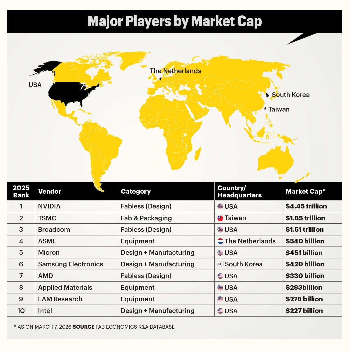
But L&T’s approach highlights a quieter reality. Fabs can cost $10–20 billion and typically operate on thin margins but design-led companies capture the bulk of the economic value. The world’s top 10 semiconductor firms have a combined market capitalisation of roughly $10.3 trillion, says US based semiconductor consultancy Fab Economics. More more than half of them derive their core value from chip design, even when manufacturing forms part of their operating model for some. Like L&T, other Indian industrial groups are tweaking their plans to de-risk and capture a bigger part of the value chain.
Enablers to Owners
The Murugappa Group initially entered the semiconductor ecosystem through testing and packaging with CG Semi. But the group soon recognised that backend capabilities alone will not deliver strategic control or long-term differentiation. The next step was chip design. This led to the creation of Axiro Semiconductor Private Ltd.
“Manufacturing is essential, but it is design and ownership of the product that determines architecture, performance, differentiation and long-term value,” says Naveen Yanduru, CEO of Axiro Semiconductor. “Over the last decade, especially post-pandemic, industries have realised that resilience is not only about fabs, it is also about owning critical design capabilities and understanding how chips integrate into real systems.”
India’s new focus on chip design builds on decades of experience in the field. Over the years, it has developed deep expertise at the foundational layer of the value chain. The country accounts for nearly one-fifth of the world’s chip design talent, which contributes to some of the most advanced microchips being produced across the world.
In February, Qualcomm of the US announced the successful tape-out of a two-nanometer (nm) semiconductor design, with the effort led in large part by its engineering teams in Bengaluru, Chennai and Hyderabad. Tape-out marks the final stage of chip design, when design data is transferred to a foundry such as Taiwan Semiconductor Manufacturing Company (TCMC) for manufacturing.
Some Indian IT companies have been providing semiconductor engineering services to global clients for decades. Yet, India’s role has largely remained that of an enabler rather than an owner. That mindset is changing now.
“At present, many Indian companies are tagged as service companies, providing human resources or services for engineering development. If you have to move out of a service mindset to a product ownership mindset, the starting point is designing an IP or a chip on your own, rather than just providing human resources for somebody else to do that,” says Navin Bishnoi, India Country Manager and Associate Vice President at Marvell India, the Indian arm of US-based chip designer Marvell Technology.
Owning the chip, instead of relying on off-the-shelf silicon, gives companies control over performance, cost, security and long-term product road maps. As systems grow more complex and software-driven, differentiation increasingly begins at the silicon layer.
“Today, to be a major player in many industries, you need custom silicon for performance, efficiency, and differentiation—especially in AI/ML (Artificial Intelligence/Machine Learning). Global players like Microsoft, Meta, and AWS have moved into chip design for that edge,” says Alok Jain, Corporate Vice President, Research and Development, Cadence Design Systems, one of the world’s top three semiconductor electronic design automation (EDA) companies.
Indian conglomerates are also recognising that they need chip design in their portfolios to build advanced systems that compete globally, he says.
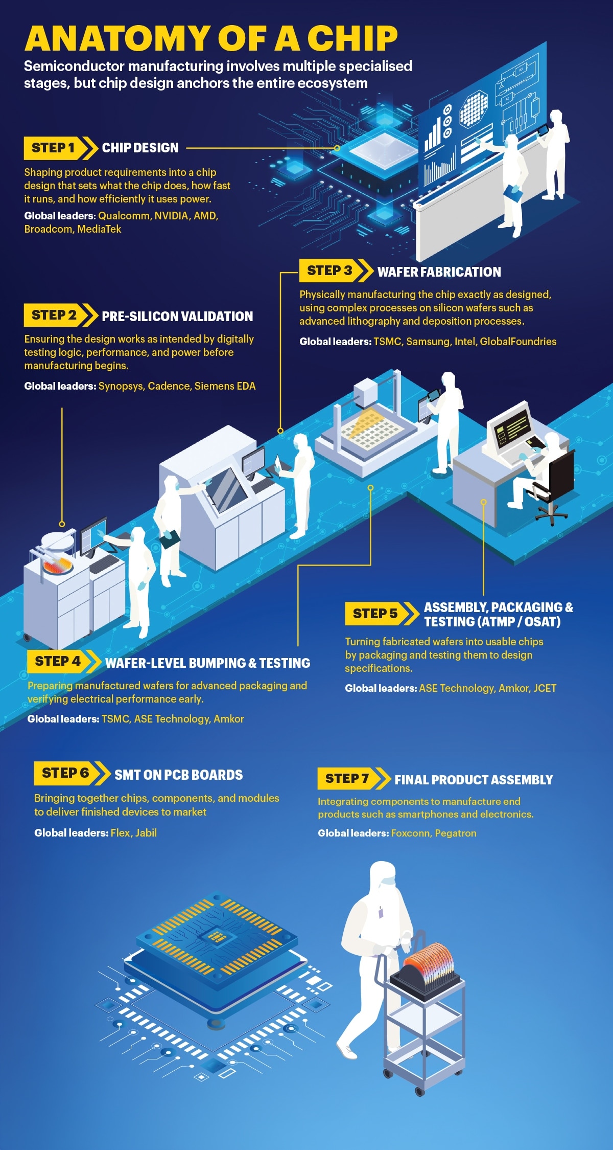
Chip design is a long-haul effort, often requiring multiple iterations before success, with each adding to research and development (R&D) costs. Once a design is finalised, companies rely on overseas foundries such as TSMC and United Microelectronics Corporation for manufacturing, resulting in long wait times between tape-out and production.
Until recently, chips designed in India were mostly fabricated in Taiwan, and tested and packed elsewhere, before being shipped back to India or to end-customers. The absence of domestic fabs and packaging facilities meant higher costs, longer cycles and limited bargaining power. This was an unviable equation in a highly cost-competitive market, say Kanishka Chauhan, Senior Principal Analyst at Gartner.
Without a fab, it was not viable for Indian companies to change their business model from design as a service company to fabless, or one that designs semiconductors and outsources production. Recent fab announcements in India are beginning to alter that by bringing the ecosystem closer home.
“Companies are no longer competing for capacity from a position of weakness, nor absorbing the cost of chips moving across multiple geographies for fabrication and packaging,” says Chauhan.

Managing Risk
Semiconductor chip design is a business that rewards patience and deep capital. It demands sustained investment in EDA tools, IP libraries, compute infrastructure and large engineering teams. Multiple design iterations, failed tape-outs, and long development cycles are common, making chip design a high-risk exercise well before manufacturing begins.
“Designing a simple power chip can cost $5–10 million for one product. But if you take a complex chip, such as a GPU (graphics processing unit) or a CPU (central processing unit), the investment can be between $200 million and even half-a-billion dollars, when you factor in tape-outs, iterations, software and validation,” says Srini Chinamilli, Co-founder & CEO of Tessolve Services, owned by Hero Electronix.
In an industry that demands sustained capital and patience, most do not survive that journey; industry estimates say nine out of ten semiconductor start-ups fail before reaching scale.
This explains why conglomerates often turn to acquisitions. Buying proven products, IP and engineering talent allows them to establish a foothold quickly and shorten the time-to-market.
For example, Axiro Semiconductor’s formation was anchored in the acquisition of the Radio Frequency component business from Japan’s Renesas Electronics Corporation, bringing a mature product portfolio, established customers and experienced engineering teams to the Indian ownership.
“We started with proven products already deployed in global networks, which significantly reduced early-stage execution risk,” adds Yanduru.
L&T has adopted a similar philosophy, albeit at a larger scale. The group has committed $300 million to get LTSCT off the ground and will continue to invest based on performance.
“When L&T Semiconductors was formed in 2023, we talked to a very broad base of customers in India, the US, Japan and Europe, to identify the product segments where they wanted to operate. During those six months, we built a team rapidly, and made one acquisition to bring in some resources and skills,” says Kumar.
Even deep pockets do not guarantee success. Ultimately, semiconductor businesses must win customers, scale volumes and compete globally on cost and performance. Here, conglomerates retain an advantage—long-standing relationships with global firms open doors for initial engagements.
L&T Semiconductors is building the business with a high level of accountability where execution and outcomes are critical. “L&T is used to building very large systems, whether it is a ship or a missile or a tank, that sell for millions of dollars. Semiconductor is the opposite end of large in terms of how much you sell, as for a single chip, $1 is a good price,” says Kumar.
Choosing The Right Battles
Today, NVIDIA is the global benchmark in semiconductor design, showing how ownership of chip architecture, software and IP creates outsize value. Indian conglomerates are not trying to replicate NVIDIA’s model nor are they attempting to compete with memory leaders such as Samsung Electronics or Micron Technology in advanced technologies such as high-bandwidth memory.
Instead, their initial focus is on semiconductor segments that are less complex, aligned with existing capabilities and offer clearer paths to customers and revenue. LTSCT, for instance, is focusing on these product areas: analog mix signals, radio frequency (RF), computing and power delivery.
Axiro Semiconductor is concentrating on high-performance RF, wireless infrastructure and satellite communication semiconductors. “These applications sit at the backbone of global connectivity, from 5G\6G radio units and fixed wireless access systems to low-earth orbit satellite terminals,” says Yanduru.
A similar approach is visible in the Tata Group. While Tata Consultancy Services (TCS) has collaborated with Tata Electronics on domestically designed chips, industry sources say these are primarily intended for internal applications, including at Tata Motors. Tata Electronics declined to comment and TCS did not respond to queries.
Starting with chips that are less complex increases the probability of success. Companies are focusing on these because they can enable this market at the fastest rate and serve a large volume of customers, says Bishnoi of Marvell India.
Given the time consumed to design chips, a company also has to ensure that the idea/chip remains relevant even after two-four years, because that’s what it will take to get the chip out and ready for someone to use, he adds. Crucially, these conglomerates are targeting distinct segments as no single company can address the market for a full range of semiconductor components.
As the India Semiconductor Mission 2.0 takes shape with a sharper focus on chip design and IP creation, the real test will be this: Can India back conglomerates willing to commit patience, capital and execution discipline that semiconductor design demands?

