
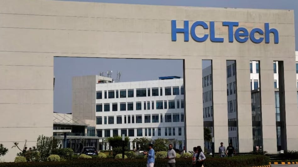
 The HCLTech lab has been equipped with testing and measurement tools from companies including Teradyne, Advantest, Keysight, Tektronix and Thermo Fisher Scientific.
IT services major HCLTech on Tuesday launched an Advanced Semiconductor Lab in Bengaluru with an investment of Rs 185 crore, expanding its capabilities in chip testing, validation and failure analysis as India seeks to deepen its role in the global semiconductor supply chain.
The 40,000 sq. ft. facility, including 25,000 sq ft of Class 10K and Class 1K cleanrooms, will offer post-silicon engineering, advanced testing and failure-analysis services. HCLTech said the facility will cater to both domestic and international customers.

 Multibagger ESDS Software shares zoom 201% from IPO price; check target price
 5 bank stocks to buy, target prices | FCNR(B) windfall, unevenly shared
  ‘Must stay the course during turbulence’: Singapore defends investment in Air India
 GST Council may take stock of one-year rate rationalisation; broad-based cuts unlikely in October meeting
 'Clear winners are NRIs and FPIs': ISB professor flags risks from RBI's $136 billion dollar strategy
 ₹1.1 Lakh Crore Defence Push: Why Stocks Are In Focus, Expert Picks Top Stocks
 Textile Stocks Surge: Why Raymond, Welspun & KPR Mills Could See More Upside Ahead
 What If The Bear Market Never Comes? Expert Explains Why Bonds Could Still Outperform Equities
 Nifty Target 25,500: Is The Next Rally The Last Before A Sharp Market Downturn?
 Apple Event Preview: iPhone 18 Pro, Foldable iPhone & New CEO?
 MTAR Technologies shares rally nearly 227% in 2026 so far; brokerage sees further upsideMultibagger ESDS Software shares zoom 201% from IPO price; check target price
 Titan, Lenskart, DMart, Trent, Meesho, Nykaa, FirstCry: Price targets, risks for consumption stocks
  Syrma SGS, Dixon, Kaynes, Avalon, Amber shares: Target prices, EMS stocks to buy
  ONGC, Oil India, Chennai Petroleum, MRPL shares climb as Brent nears $100
 China honours scientists on giant billboards. Ex-CEA wants India to honour its own greats
 Forget car factories: China's Xpeng is building a factory where robots make robots₹1.1 Lakh Crore Defence Push: Why Stocks Are In Focus, Expert Picks Top Stocks
 AI job shift: Agentic AI engineers emerge as the hottest tech hire, demand up 260%Textile Stocks Surge: Why Raymond, Welspun & KPR Mills Could See More Upside Ahead